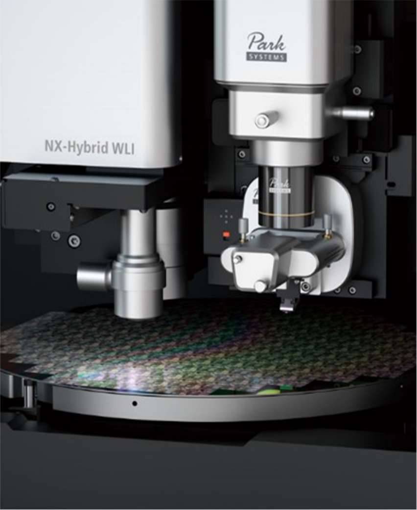

The fully automated
industrial WLI-AFM
system
Park NX-Hybrid WLI is the first-ever AFM with built-in
WLI profilometry for semiconductor and related
manufacturing quality assurance, process control for
semiconductor front-end, back-end up to advanced
packaging, and R&D metrology. It is for those that
require high throughput measurements over a large
area that can zoom down to nanometer-scale
regions with sub-nano resolution and ultra-high
accuracy.
-
Park NX-Hybrid WLI is the first ever AFM system
with built in White Light Interferometer
profilometry for R&D metrology, process control,
and manufacturing quality assurance of semiconductor devices. -
Park NX-Hybrid WLI provides high throughput
imaging over a very large area with the WLI
module, and nanoscale metrology with
sub-angstrom height resolution over the areas of
interest using AFM. -
Park NX-Hybrid WLI offers the ultimate solution,
ranging from large area scanning to nanoscale
metrology, for various applications including
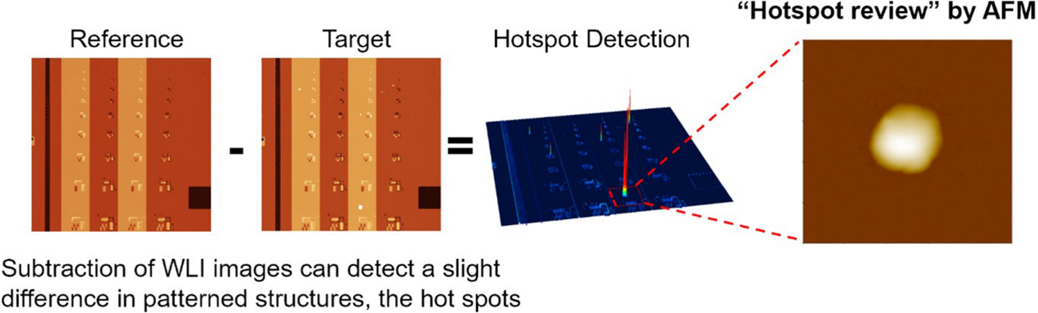
quality assurance, automatic defect review,
front-end semiconductor process control,
and back-end advanced packaging. -
Park NX-Hybrid WLI seamlessly integrates an
automated industrial AFM system and a WLI
profilometer, bringing significant cost savings,
reduced tool footprint, and new metrology
solutions compared to the previous two tool solution.
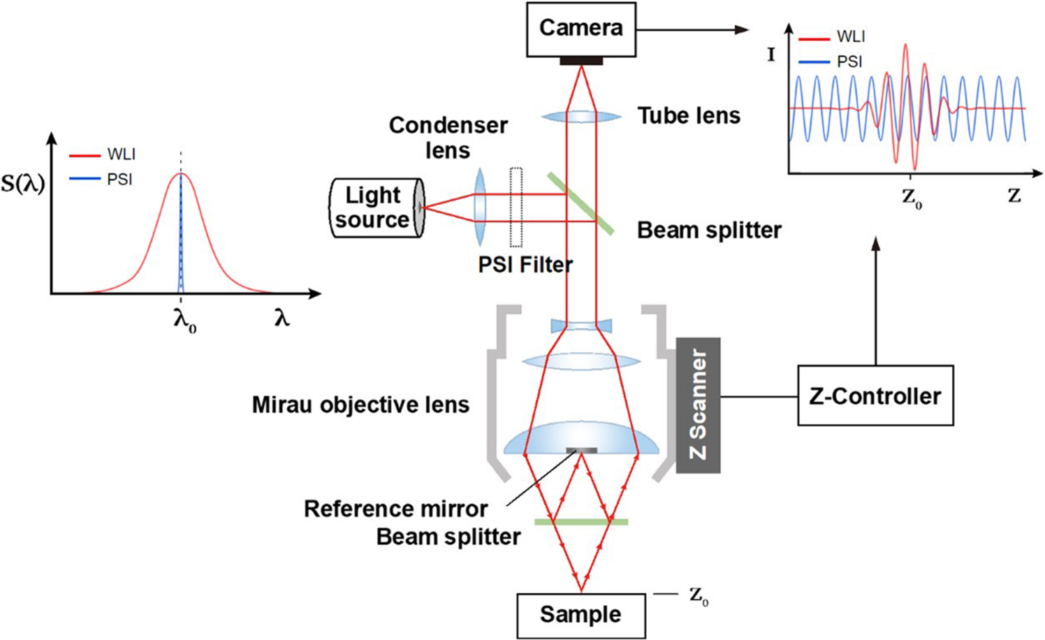
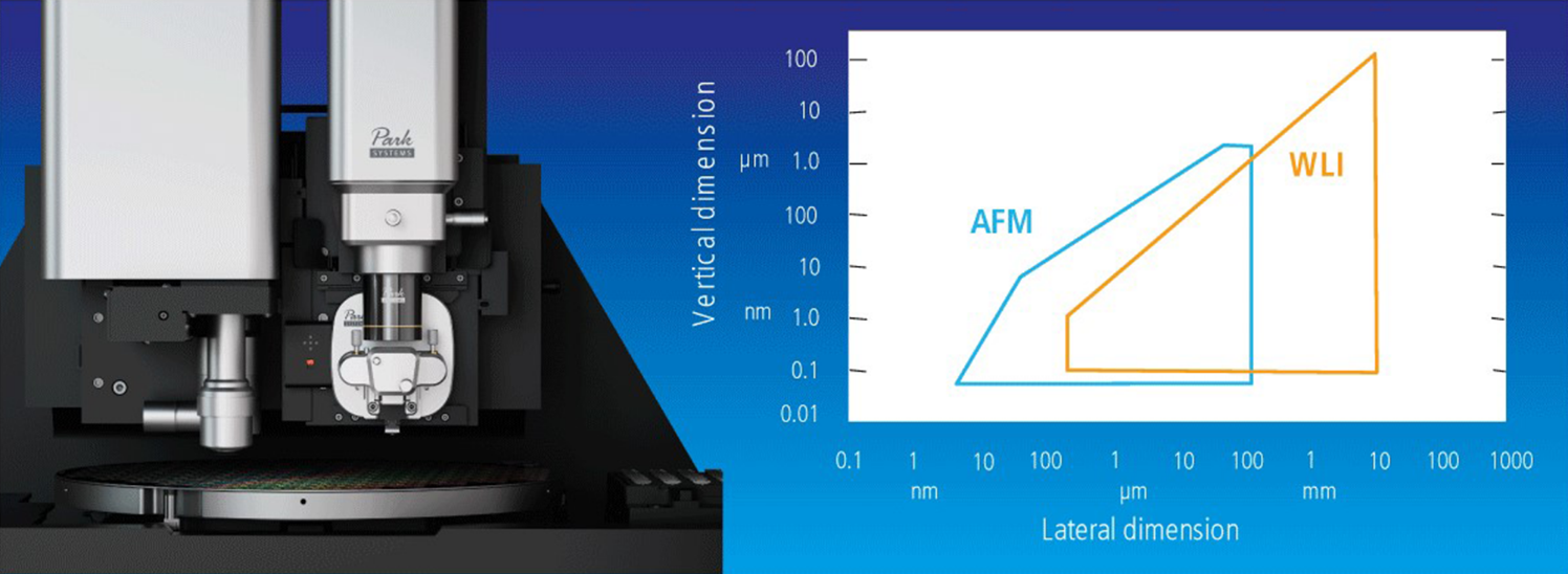
The two best
complementary
technologies for
semiconductor metrology
-
WLI : White light interferometry is an optical
technique that can image a very wide area, very
fast, producing high throughput measurements. -
AFM : Atomic force microscopy is a scanning probe
technique that delivers the highest nanoscale
resolution measurements even for transparent materials.
| WLI | AFM | |
|---|---|---|
| Measurement Area | Large | Small |
| Speed | High | Low |
| Lateral Resolution | Low | High |
| Vertical Resolution | High | Very High |
| Accuracy | Low | High |
WLI and AFM complement each other in field of
view, resolution, and speed
WLI applications requiring much
higher resolution and accuracy
beyond WLI capability
- WAdvanced CMP metrology and monitoring
- Advanced packaging
- Hot-spot and defect detection on full reticle die
- Wafer level metrology
AFM applications requiring much
higher throughput over much larger
areas
- In-line Wafer Metrology
- Long Range Profiling for CMP Characterization
- Sub-Angstrom Surface Roughness Control
- Wafer Inspection and Analysis