The leading nano
metrology tool for failure
analysis and large sample
research
FA 엔지니어라면 누구나 정확하며 오차가 없는 데이터 값을 얻을 수 있는 장비를 원하실 것입니다. Park Systems의 NX20은 세계에서 가장 정확한 대형 시료용 AFM 이며, 반도체와 하드디스크 산업에서도 가장 정확한 결과 산출을 할 수 있습니다.
More powerful failure analysis
solutions
Park Systems의 NX20은 디바이스의 결함을 발견하고 독창적인 결과물을 개발하는 것을 좀더 쉽게 하는 고유의 특징들을 갖추고 있으며, 사용자가 NX20이 제공하는 고해상도 데이터로 프로젝트를 더욱 수월하게 해결 할 수 있게 도와줍니다. 또한 NX 20의 완전 비접촉 모드™ 는 팁을 날카롭고 수명을 길게 유지 시켜주기 때문에 장시간 고해상도 스캔이 가능하며 팁을 교체하는데 드는 시간과 비용을 절약 할 수 있습니다.
Easy to use, even for entry level
engineers
Park Systems의 NX20은 다루기 쉬운 디자인 과 자동화 인터페이스를 가지고 있기 때문에 사용자는 장비를 사용하거나 신입 엔지니어를 교육하는데 많은 시간과 에너지를 쓸 필요가 없습니다. 이것은 사용자가 더 큰 문제를 해결하는 것과 고객에게 좀더 정확한 분석 데이타를 제공할 수 있습니다.
Accurate AFM Solutions
for FA and Research
Laboratories
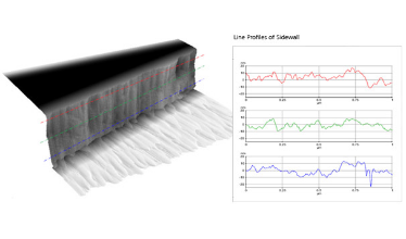
Sidewall measurements for
3D structure study
NX20의 획기적인 구조로 인하여 샘플의 측벽과 표면을 탐지하고 각각의 각도를 측정하는 것이 가능합니다. 이것은 사용자가 혁신적이고 깊이있는 연구를 할 수 있도록 도와줍니다.
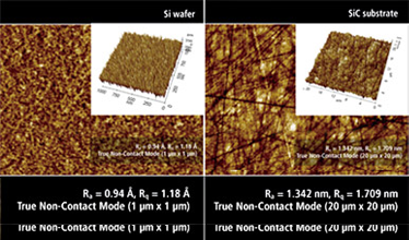
Surface roughness measurements for
media and substrates
표면 거칠기 측정은 NX20의 핵심 기능 중의 하나이며, NX20은 정확한 고장분석과 품질보증을 제공합니다.
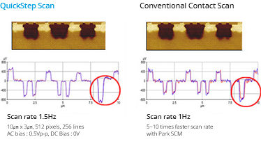
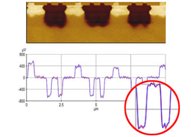
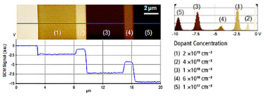
High resolution electrical scan mode
QuickStep SCM
가장 빠른 전기용량 측정 원자현미경
PinPoint AFM
마찰이 없는 전도성의 AFM
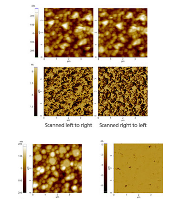
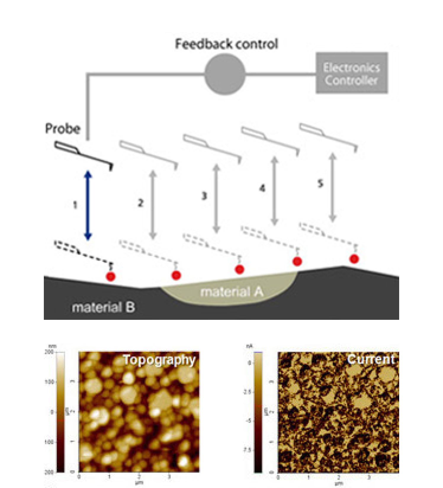
Accurate AFM Scan by
True Non-Contact™ Mode
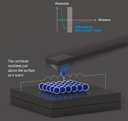
True Non-Contact™ Mode
True Non-Contact™ Mode is a scan mode unique
to Park AFM systems that produces high resolution
and accurate data by preventing destructive tip-sample
interaction during a scan.
Accurate Feedback by Faster Z-servo enables
True Non-Contact AFM
-
Less tip wear → Prolonged high-resolution scan
-
Non-destructive tip-sample interaction → Minimized sample
modification
-
Maintains non-contact scan over a wide range of samples
and conditions
Unlike in contact mode, where the tip contacts
the sample continuously during a scan, or in
tapping mode, where the tip touches the sample
periodically, a tip used in non-contact mode does
not touch the sample. Because of this, use of non-contact
mode has several key advantages.
Scanning at the highest resolution throughout
imaging is now possible as the tip’s sharpness is
maintained.
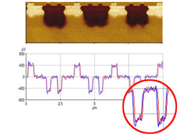
Accurate AFM
Topography with
Low Noise Z Detector
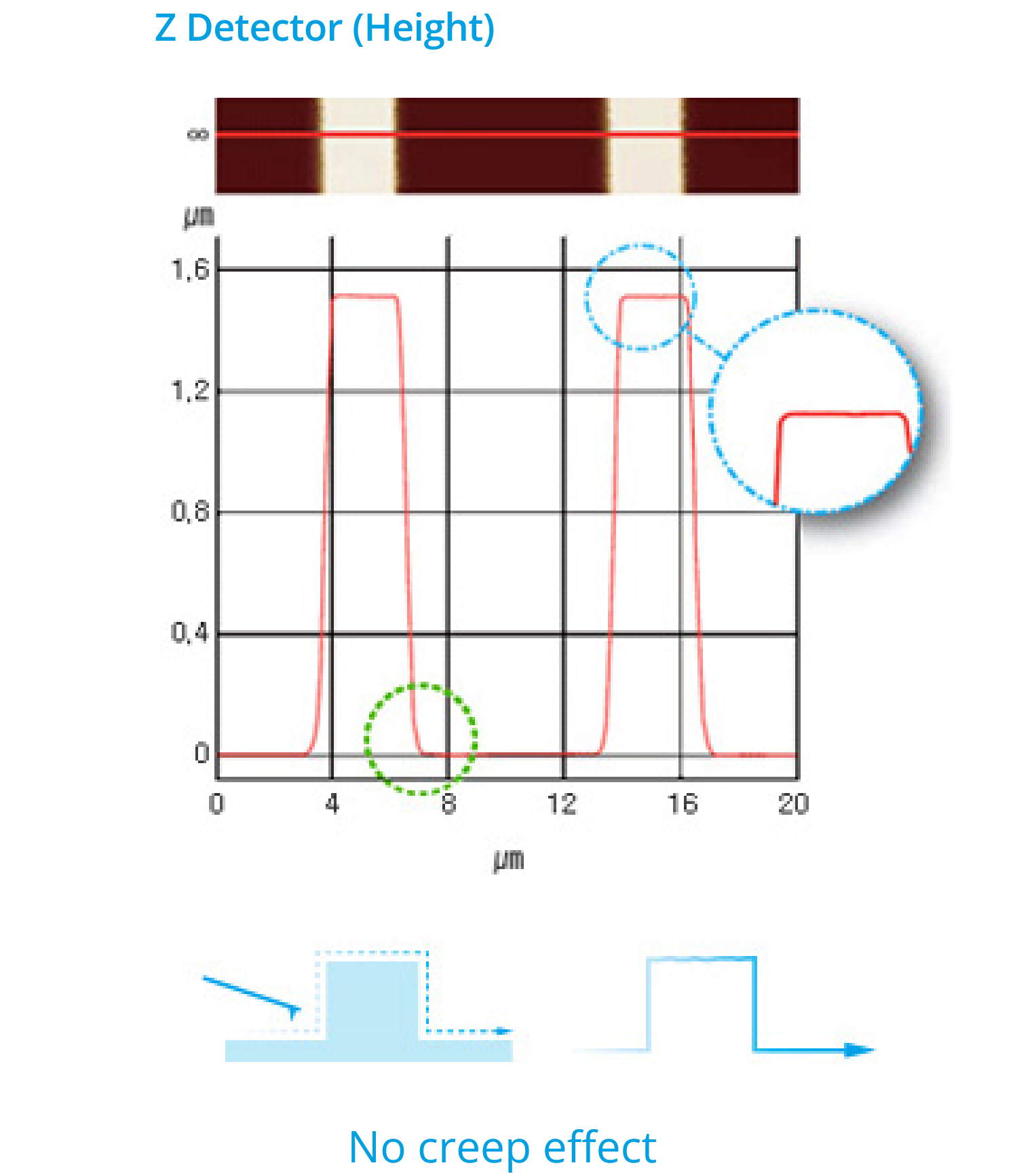
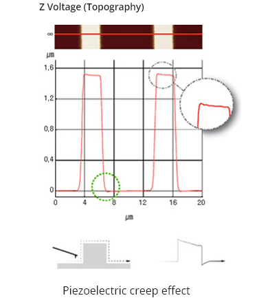
True Sample Topography™
without piezo creep error
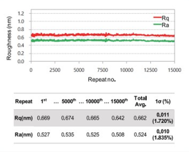
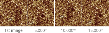
Park Systems의 AFM은 가장 효과적인 저 노이즈Z검출기로 0.02nm이상의 넓은 대역폭은 가집니다. 이는 정확하게 샘플의 형상도를 측정할 수 있으며, 모서리의 측정 오류가 없어 별도의 측정이 필요하지 않습니다. 또한 시간단축을 해주고 더 좋은 정보를 얻을 수 있습니다.
-
Low noise Z detector signal is used for topography
-
Low Z detector noise of 0.02 nm over large bandwidth
-
No edge overshoot at the leading and trailing edges
-
Calibration needs to be done only once at the factory