Park NX-Wafer

Low Noise, High Throughput Atomic Force
Profiler with Automatic Defect Review

Scan range

XY Scan Range: 100X100 µm,
Z Scan Range: 15 µm

Sample size

200 mm / 300 mm Wafer

Low Noise, High Throughput Atomic Force Profiler

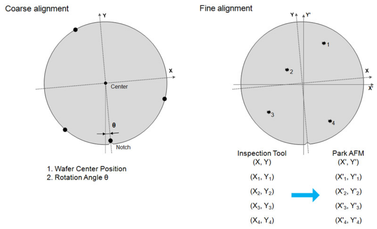
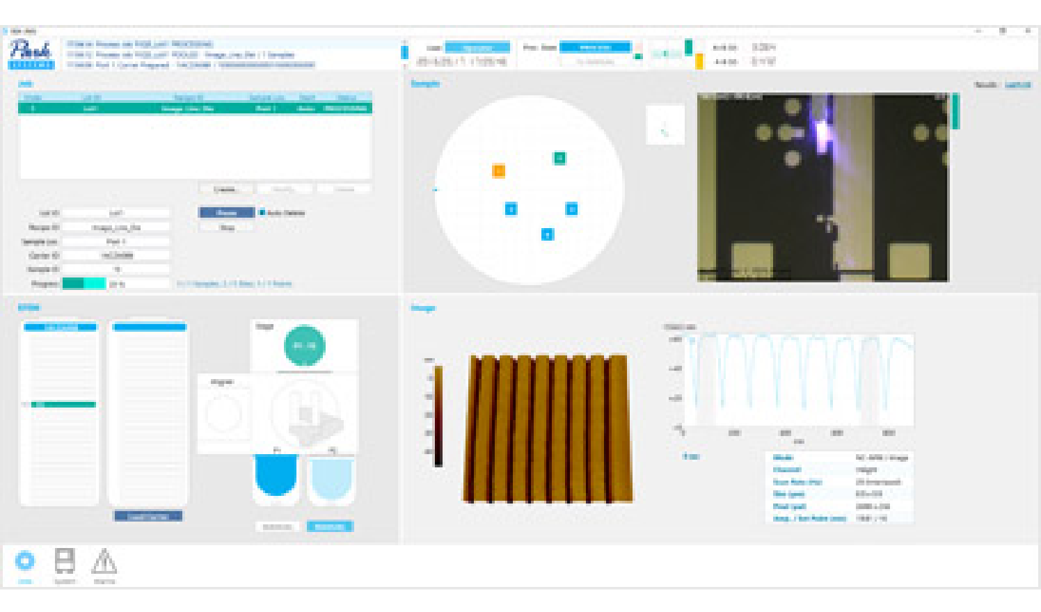
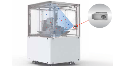
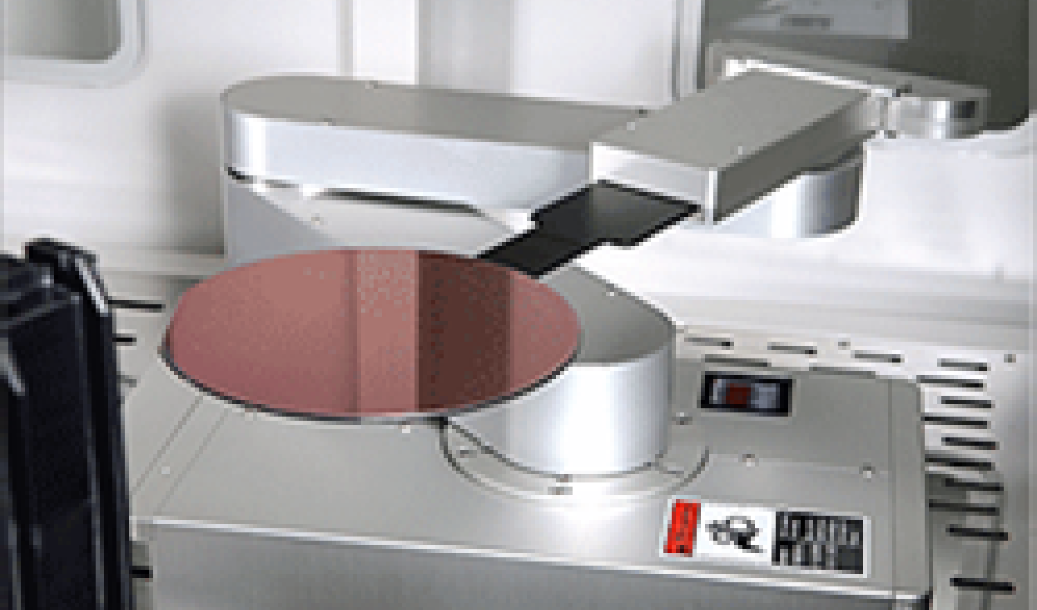
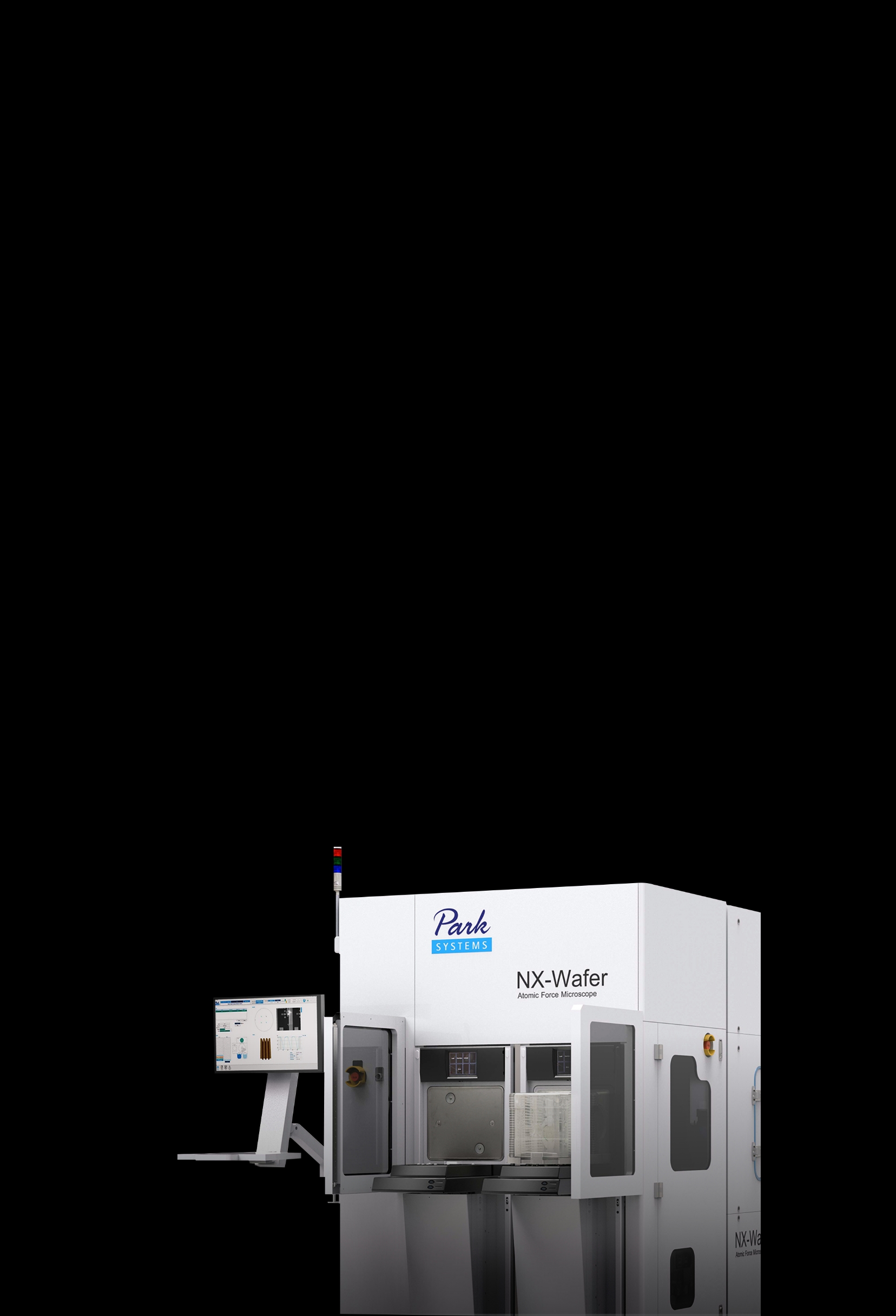
Park NX-Wafer is the industry’s leading automated AFM metrology system for semiconductor and related fabrications. It provides wafer fab inspection and analysis, automatic defect review for bare wafers and substrates, and CMP profile measurements. Park NX-Wafer has the highest nanoscale surface resolution with sub-angstrom height accuracy, scan after scan with negligible tip to tip variation and preserved tip sharpness unmatched by others. Park NX-Wafer with its automated system features including auto tip exchanger, live monitoring, target positioning without reference marks and auto analysis makes the best semiconductor AFM tool in the industry.

  • Low noise atomic force profiler for more accurate CMP profile measurements
  • Sub-Angstrom surface roughness measurements with extreme accuracy and negligible tip-to-tip variation
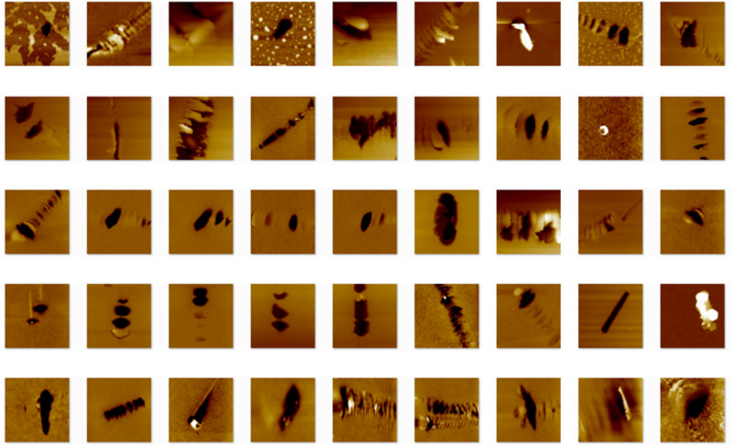
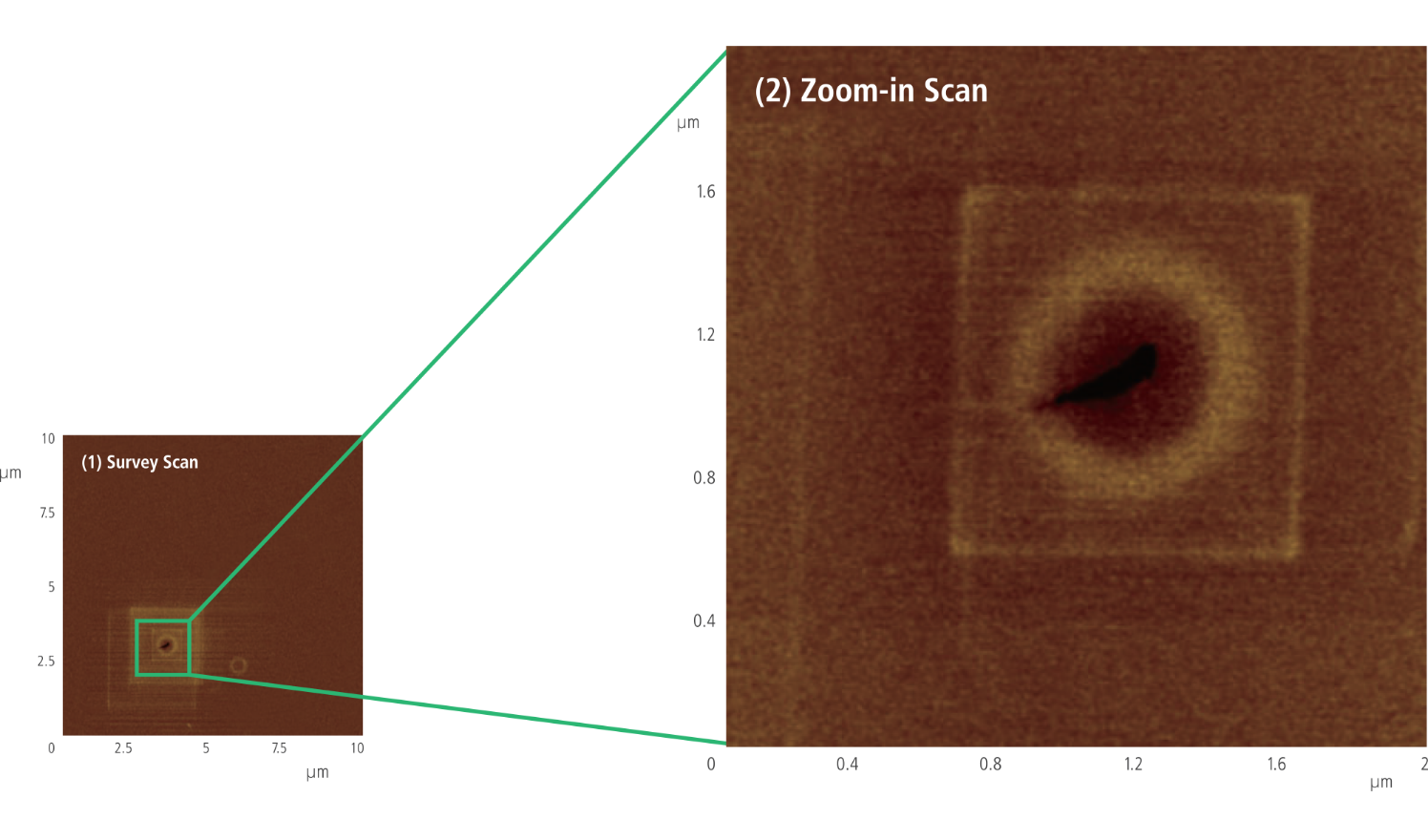
  • Fully automated AFM solution for defect imaging and analysis
  • A fully automated system with auto tip exchange, robot wafer handler
  • Capable of scanning 300 mm wafers

A revolutionary all-in-one system for 3D Metrology

High productivity and
powerful features
for inline wafer-fab
metrology

Automatic Defect Review for Bare Wafers and Substrates

The new 300mm bare wafer ADR provides a fully
automated defect review process from transfer
and alignment of defect maps to the survey and
zoom-in scan imaging of defects that uses a
unique remapping process that does not require
any reference marker on a sample wafer. Unlike
SEM which leaves square-shaped destructive
irradiation marks on defect sites after its run, . the
AFM-based defect review enables non-destructive
3D imaging of defects as small as a few
nanometers. The linkage between a defect
inspection tool and the AFM is carried out by
advanced coordinate translation with enhanced
vision technique. Since it is fully automated,
it does not require any separate steps to calibrate
the stage of the targeted defect inspection system,
increasing throughput by up to 1,000%.

Automatic Transfer and Alignment of Defect Maps with Enhanced Vision

By utilizing Park's proprietary coordinate
translation technique, the new Park ADR AFM can
accurately transfer the defect maps obtained from
a laser-scattering defect inspection tool to a
300mm Park AFM system.
This technology does not require any separate
step to calibrate the stage of the targeted defect
inspection system and allows full automation for
high throughput defect imaging.

Automated Search & Zoom-in Scan

The defects are imaged in two steps;(1) a survey
imaging, either by AFM or enhanced optical vision,
to refine the defect location, then (2) a zoom-in
AFM scan to obtain a detailed image of the defect,
presenting automatic analysis of the defect type
and the subsequent defect dimensions.

Long Range Profiling for CMP
Characterization

Planarization is the most important step in the
back-end processes where metals and dielectric
materials are used. Both local and global
uniformity after chemical mechanical polishing
(CMP) affect the yield of chip manufacturing
significantly. Accurate CMP profiling is a critical
metrology necessary to optimize process
conditions for best planarity and improve
production yield.

Combining Park NX-Wafer with a sliding stage
provides a long range profiling capability for CMP
metrology. Due to the unique scanner design
of Park's automated AFM, the combined system
provides very flat profiling and there is no
need for complex background subtraction or calibration
after each measurement. The Park NX-Wafer
enables unprecedented CMP metrology of both
local and global planarity measurements including
dishing, erosion, and edge-over-erosion (EOE).

Sub-Angstrom Surface Roughness
Control

Semiconductor suppliers are developing ultra-flat
wafers to address the ever-increasing need for
shrinking device dimensions. However, there has
never been a metrology tool capable of providing
accurate and reliable measurements for the sub-Angstrom roughness of these substrate surfaces.
By delivering the industry's lowest noise floor of
less than 0.5 Å throughout the wafer area, and
combining it with True Non-Contact™ Mode™, the
Park NX-Wafer can make accurate, repeatable, and
reproducible sub-Angstrom roughness
measurements for the flattest substrates and
wafers with minimized tip-to-tip variation.
Very accurate and repeatable surface
measurements can be obtained even for the long-range waviness measurement of scan sizes up to 100m x 100m.

High-Throughput Wafer-Fab
Inspection and Analysis

  • Automatic tip exchange with 99.9% success rate and minimum tact time
  • Equipment Front End Module (EFEM) for automatic wafer handling
  • Cleanroom compatibility and remote control interface
  • Automatic data acquisition and analysis of trench width, depth, and angle measurements

Park NX-Wafer features

The long range profiler is an essential component of Atomic Force Profilometry (AFP) and comes with a dedicated user interface for the automated CMP profiling and analysis.

  • 200mm : 10 mm
  • 300mm : 25 mm (optional 10 mm or 50 mm)

The XY scanner consists of symmetrical 2-dimensional flexure and high-force piezoelectric
stacks that provide highly orthogonal movement
with minimal out-of-plane motion, as well as the
high responsiveness essential for precise sample
scanning at the nanometer scale. Two symmetric,
low-noise position sensors are incorporated on
each axis of the XY scanner to retain a high level of
scan orthogonality for the largest scan ranges and
sample sizes. The secondary sensor corrects and
compensates for non-linear and non-planar
positional errors caused by a single sensor alone.

The NX-Wafer provides you with unprecedented
accuracy in topography height measurement by
utilizing its ultra-low noise Z detector instead of the
commonly used Z voltage signal that is non-linear
in nature. This industry leading low noise Z
detector replaces the applied Z voltage as the
topography signal.

The NX-Wafer is equipped with automated
software that makes operation nearly effortless.
Just select the desired measurement program to
get precise multi-site analysis with optimized
settings for cantilever tuning, scan rate, gain, and
set point parameters.

Park's user-friendly software interface gives you
the flexibility to create customized operation
routines so you can access the full power of the
NX-Wafer and get the measurements you need.

Creating new routines is easy. It takes about 10
minutes to make one from scratch, or less than 5
minutes to modify an existing one.

  • Auto, semi-auto, and manual mode so you have complete control
  • Editable measurement method for each automated routine
  • Live monitoring of the measurement process
  • Automatic analysis of acquired measurement data

Automatic Tip Exchange (ATX)

The ATX automatically locates tips by pattern
recognition and uses a novel magnetic approach to
disengage a used tip and pick up a new tip, with an
incredible 99.9% success rate. The laser spot is
then automatically optimized along the X- and Y-axis by motorized positioning knobs.

Ionization System for a more stable scanning environment

Our innovative ionization system quickly and
effectively removes electrostatic charges in your
sample's environment. Since the system
always generates and maintains the ideal balance
of positive and negative ions, it can create an
extremely stable charge environment with little
contamination of the surrounding area and
minimal risk of accidental electrostatic charge during sample handling.

Automatic Wafer Handler
(EFEM or FOUP)

The NX-WAFER can be configured for various
automatic wafer handlers (EFEM or FOUP or
other). The high-precision, nondestructive wafer
handler robot arm fully ensures users always get
fast and reliable wafer measurements.